
SK Hynix, one of the world's leading high-bandwidth memory (HBM) makers, has begun construction of its first United States facility in Indiana, with CEO Kwak Noh-Jung saying the site will make the state a “key HBM production base in America” by 2030.
Speaking at a groundbreaking ceremony in West Lafayette on Thursday, Kwak highlighted the growing demand for HBM as artificial intelligence development drives a critical global shortage of advanced memory.
“We will provide our customers with a new source of made-in-U.S. HBM, while strengthening the U.S. semiconductor supply chain and contributing to national and economic security,” Kwak said.
SK Hynix is the market leader in HBM and is in the midst of a $720 billion expansion programme to increase production, with most of the investment taking place in South Korea, where the company is building the world's largest memory fabrication campus. Production there is scheduled to begin in February.
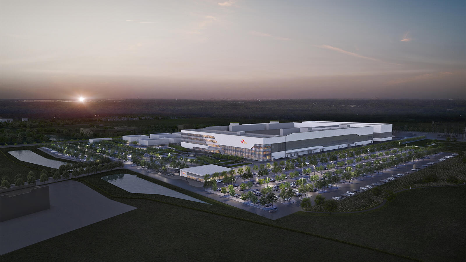
The $4 billion Indiana facility will focus on packaging rather than front-end chip manufacturing. Memory chips produced in South Korea and China will be shipped to Indiana, where they will be stacked and connected.
The first cleanroom at the facility is scheduled to open in October 2028, Kwak said.
While packaging is a critical stage of semiconductor production, US Commerce Secretary Howard Lutnick called on SK Hynix and rival Samsung in July to build front-end chip fabrication plants in the US.
Kwak said SK Hynix is searching for the right opportunity and is “open to every site or every country”. He added: “SK Hynix will continue to expand its investment and cooperation in America.”
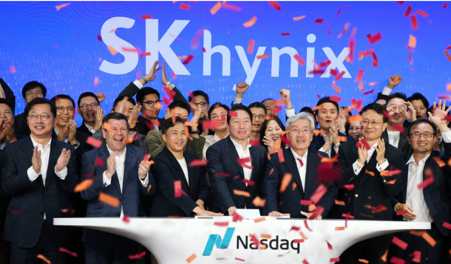
SK Hynix, which trades on the Korea Exchange, listed shares on the Nasdaq in July, raising $26.5 billion, the largest U.S. market listing by a foreign company. The stock has been volatile amid swings in AI-related shares and the broader Korean market.
Despite this, SK Hynix's market capitalisation has increased about sevenfold over the past year to more than $1 trillion.

SK Hynix began construction at the Indiana site in April, with Thursday's event formally marking the start of the project. Indiana Governor Mike Braun described it as the “biggest development project in Indiana’s history” and the “first of its kind in the country”.
“For too long, the United States designed many of the world’s most advanced chips, while allowing too much of the manufacturing ecosystem to migrate overseas,” Indiana State Senator Todd Young said. “Breaking ground here today is evidence that that vision is being realised.”
Kwak said SK Hynix's total U.S. investments and assets are expected to exceed $45 billion by 2030.
This includes a $10 billion “AI Company” launched in January and subsidiary Solidigm, which SK Hynix acquired from Intel's NAND business for $9 billion in 2020.
SK Hynix will receive up to $458 million in federal CHIPS Act funding and a state incentive package worth up to $712 million, according to the Indiana Economic Development Corporation.
Announced in 2024, the 133-acre site will include the packaging facility and research and development centres where major AI customers can work with SK Hynix on new memory technologies.
Nvidia, the world's leading AI chipmaker, has committed to co-developing memory with SK Hynix as part of a $500 billion deal with SK Group announced in July.
SK Hynix said the Indiana facility will create around 1,000 direct jobs, alongside a further 6,000 construction and business partner positions.
Initially, employees from South Korea will be temporarily relocated to support the project, while long-term roles are expected to be filled by U.S. workers, including graduates from nearby Purdue University, which offers semiconductor-focused degrees.
“In 167 years at Purdue University, there has not been a bigger day than today,” Mitch Daniels, Purdue's interim president and former governor of Indiana, said on Thursday.